
Author: Godot
In 2012, the world's largest DRAM memory manufacturer went bankrupt.
This Japanese company called Elpida was once the pride of Japan's semiconductor industry, backed by the technological accumulation of giants like NEC, Hitachi, and Mitsubishi, but even with government investment, it could not survive.
With debts of 430 billion JPY, it filed for bankruptcy protection and was subsequently acquired by a U.S. company for 200 billion JPY. It integrated, digested, and completely disappeared from history. That U.S. company was Micron Technology.
Intel has made DRAM, but exited. Texas Instruments has done so, but exited. Motorola has done so, but exited. The entire Japanese semiconductor memory industry went from peak to collapse in less than twenty years. The Koreans took up the baton, with Samsung and SK Hynix sweeping the market with government subsidies and aggressive price wars, pushing all competitors to the wall.
Micron survived and has become the only company in the United States capable of mass-producing advanced memory chips today.
This company based in Boise, Idaho, operates in the shadow of Nvidia and TSMC. It does not design GPUs and does not manufacture logic chips.
But as AI pushes the world's hunger for computational power to the limit, a previously overlooked physical bottleneck has suddenly become unavoidable— the time the computing unit spends waiting for data is longer than the computation itself.
This problem has no software solution, only a hardware solution. And that hardware happens to be what Micron has been doing for forty years.
1. Physical and System Limits of AI Computing
Revisiting the Memory Wall
Under the current von Neumann architecture, GPU or TPU computing units are physically independent from main memory.
Inside the computing unit, there is a small amount of SRAM (Static Random-Access Memory) as on-chip cache.
Model weights and input data are mainly stored in off-chip DRAM (Dynamic Random Access Memory).
Data must be transferred between the two in the form of electrical signals through intermediary physical structures.
For example, a large language model with 70 billion parameters requires approximately 140GB of physical memory just for the weight data itself at FP16 precision.
Current mainstream high-end AI computing cards have video memory capacities between 80GB and 192GB, and models of slightly larger size must be split across multiple cards to run.
In the past decade, chip computing power has improved exponentially. However, memory bandwidth growth is constrained by the number of physical pins, signal frequency, and heat dissipation limits, lagging far behind computing power.
When computing speed exceeds memory supply speed, the computing unit is forced into a waiting state, leading to a significant drop in the utilization of expensive hardware.
Training and Inference
Training and inference are two phases of AI. Training is to refine the accuracy of large models, taking place in the background. Inference is the process of generating results when users interact, taking place in the foreground.
The characteristic of training is batch parallel processing.
The same batch of data is repeatedly used in the computing core's cache, resulting in high arithmetic intensity; the system is mainly limited by computing speed rather than memory. This scenario highlights Nvidia’s strength in computing power.
Inference, however, is a different matter. Large language models generate text based on an autoregressive mechanism.
Each time it outputs only one token, which is then used as input for the next step. To avoid recomputing previous attention scores for each generation, the system maintains a KV Cache in the video memory to store the key-value tensors of historical sequences.
At a context length of 4096, a single user request requires about 1.34GB of video memory. If we deduct the memory weight usage from the two A100 cards, about 20GB remains available for the KV Cache, which can support a maximum of approximately 14 concurrent requests.
During inference, the arithmetic intensity is extremely low, and the system is completely limited by memory bandwidth, making it a memory-intensive task. The real determinant of throughput limits is the physical transfer rate of HBM.
In terms of energy consumption, the energy cost of reading data from off-chip HBM is about 10–20 pJ/bit, while executing a single FP16 floating-point operation only requires about 0.1 pJ. The energy used to move data is 100 to 200 times that of the computation itself.
In large-scale inference scenarios, if the memory access pattern is not optimized, data center power will be consumed largely in bus transmission rather than actual logic calculations.
This is precisely the physical driving force behind Micron's continuous advancement of HBM technology.
2. Analysis of Micron's Core Semiconductor Technology
First, what kind of company is Micron Technology?
Micron is an IDM integrated device manufacturer, handling everything from design, manufacturing, to packaging.
However, Micron's fabs only produce one thing: memory chips. It does not make CPUs, nor GPUs, only memory and flash memory.
In terms of product structure, Micron's revenue can be roughly divided into three parts. DRAM accounts for more than 70%, NAND accounts for two to three tenths, and NOR flash memory accounts for a smaller proportion.
DRAM refers to the memory sticks we're familiar with; NAND is the core medium of solid-state drives; NOR is mainly used in automotive electronics and industrial equipment, executing startup codes quickly, having low presence but being irreplaceable.
In terms of the end market, Micron has four business divisions: the computing and networking division for data centers and servers, the mobile division for smartphones, the solid-state drive division for enterprise storage, and the embedded division for automotive and industrial applications.
What role does Micron play in the AI supply chain?
Nvidia makes GPUs, TSMC provides foundry services; where does Micron fit into this chain?
In simple terms, Nvidia's H100 and B200 GPUs are manufactured by TSMC, and Micron is not involved in this segment. However, a complete accelerator card capable of running large models requires more than just computing cores. As previously explained, the performance bottleneck during inference lies in memory bandwidth, not computing power itself.
Therefore, Nvidia must tightly integrate high-bandwidth memory HBM next to the GPU. These HBMs are produced by Micron (as well as SK Hynix and Samsung) and then packaged together with the GPU logic chip on the same silicon interposer through TSMC’s CoWoS advanced packaging technology to form a complete AI computing module.
Micron is a key component supplier. The GPU is the brain, while the HBM is the ultra-high-speed data channel closely tied to the brain; both are indispensable.
This structure means that Micron's competitive logic is entirely different from Nvidia's. Nvidia builds its moat based on architecture and ecosystem, while Micron relies on continuous iteration of process technology and stacking packaging techniques.
The bandwidth improvement of each generation of HBM is backed by more complex TSV (Through-Silicon Via) technology and higher stacking layers, making the hurdles not low.
DRAM: The Infrastructure Hidden Behind Compute Power Narrative
Before the advent of AI computing power, there was a more fundamental question: where does the data come from, and how does it reach the computing core? The answer to this question is DRAM (Dynamic Random Access Memory).
Starting with personal computers
DRAM is the main memory in traditional computers, solving speed mismatch issues.
Hard drives can store a lot but are slow to read. CPUs can calculate quickly but have no place to temporarily hold data. There’s a speed difference of three orders of magnitude between them. A CPU waiting for a hard drive is like driving on a highway behind a tractor.
DRAM resolves this issue. When a user opens a program, the operating system moves its code and data from the hard disk into DRAM;
the CPU then sends address commands directly to DRAM, completing read and write operations with nanosecond-level latency and tens of GB/s bandwidth. The operating system’s kernel, the state of background processes, everything currently running, all reside here in real-time.
Loss of power means loss of data; this is also the meaning of the word "dynamic," as the capacitance of DRAM naturally leaks electricity and needs continuous refreshing to maintain data.
Physically, each storage cell in DRAM consists of one transistor and one capacitor (1T1C).
As we enter the AI scenario, the nature of the demand changes.
The AI computing core shifts from the CPU to the GPU. The form of DRAM also evolves, no longer just DDR memory sticks plugged into motherboards, but instead as HBM high-bandwidth memory, vertically stacked in multiple layers of bare chips through TSV technology, packaged on the same interposer as the GPU.
The demand for DRAM also transforms from merely supporting system operations to breaking through compute power bottlenecks.
First is the loading of model weights. The parameters of large models are stored in matrix form in physical memory and must all reside in the HBM close to the computing core before inference begins. A 70 billion parameter model, in FP16 format, requires about 140GB of storage space for the weights alone.
Secondly, there is the dynamic occupation of the KV Cache. When a model generates text, it needs to reference all previous context for each word it outputs.
To avoid recalculating everything each time, the system caches the history in the video memory, which is the KV Cache.
The longer the context, the larger the cache. Two A100 cards, minus the footprint used for model weights, leave enough video memory to only simultaneously serve a dozen users. This is the actual concurrency limit for a server costing tens of thousands of dollars.
The consumption is greater in training scenarios. Training not only needs to store model parameters but also retains intermediate computation results for each layer for easy weight updates during backpropagation.
Commonly used Adam optimizers will also keep two extra records for each parameter. Altogether, the video memory used during training is often three to four times that used during inference.
This brings us back to the memory wall issue. The computing power of the GPU cores increases far more rapidly than memory bandwidth does. The arithmetic intensity during inference is extremely low, and the GPU spends much of its time waiting for data.
Each generation's bandwidth improvement of HBM directly determines the actual throughput limits that AI inference servers can support.
This is the core value of DRAM in the AI era and the underlying logic behind Micron's continual investment in HBM research and development.
Three Oligarchs: Where Does Micron Rank?
In the global DRAM market, Samsung, SK Hynix, and Micron together account for about 95% of the share. However, each has completely different strengths.
Process Advancement: Micron is Faster
In semiconductor manufacturing, the process (Process Node / Technology Node) refers to the feature size of the micro-physical structures inside integrated circuits.
When assessing that Micron is moving fastest in process advancement, it means Micron is leading in shrinking the physical structures within DRAM chips and improving storage density per unit area, ahead of Samsung and SK Hynix.
In other words, each wafer can yield more chips, reducing the manufacturing cost per bit, supporting higher profit margins.
From 1-alpha to 1-beta and further to 1-gamma, Micron is usually the first to announce mass production of a new generation of high-density DRAM.
Samsung has encountered yield bottlenecks below the 14nm node, and the pace of deliveries has noticeably slowed in the recent two generations. SK Hynix's process advancement speed is approximately comparable to Micron's, with both being in the same tier.
HBM: Hynix’s Home Ground
Process is Micron’s strength, but the HBM market is currently home ground for SK Hynix.
Hynix holds more than 50% of the HBM market share and is the exclusive supplier for Nvidia's highest-tier GPUs. Its core technology advantage lies in the MR-MUF packaging process, which excels in heat dissipation and yield control when stacking multiple DRAM bare chips.
Micron is a latecomer, skipping HBM3 and going straight to HBM3E, leveraging efficiency advantages to enter Nvidia's supply chain. However, it uses TC-NCF packaging, which poses higher manufacturing difficulties for multilayer stacking, making overall capacity and market share lag behind Hynix clearly.
Samsung, on the other hand, has another story. At the HBM3 and HBM3E stages, Samsung's products failed to timely pass Nvidia's tests due to heat and power consumption issues, missing the concentrated time window of this round of AI memory boom. Currently, it is betting on a comeback during the HBM4 stage.
Energy Efficiency: Micron's Differentiation Cut
While Micron's market share in the HBM market lags behind Hynix, its differentiation lies in power consumption.
Public testing data shows that Micron's HBM operates with about 20% to 30% lower running power than competing products while providing the same data bandwidth. This number may seem small for a single GPU but translates directly into electricity costs in a data center deploying tens of thousands of GPUs.
Currently, the electricity supply and cooling of AI data centers have become expansion bottlenecks, and energy efficiency metrics are increasingly affecting procurement decisions.
The same logic extends to mobile. Micron's LPDDR5X based on the 1-gamma process reaches speeds of 9.6Gbps while reducing overall power consumption by 30%. Running local AI models in mobile devices, battery life is an indicator that users can directly perceive.
Scale: Samsung's Ace
Micron’s overall production capacity is the smallest. Lacking the absolute scale of Samsung, Micron cannot rely on price wars and can only take the technology premium route.
This is also why Micron must stay ahead in process and energy efficiency; once the technological advantage disappears, it stands no chance in price competition.
To summarize the positions of the three companies:
Hynix has captured the largest portion of AI memory profits through HBM packaging technology; Samsung maintains dominance in the conventional DRAM market due to scale, but has faltered in HBM; Micron leads in process and energy efficiency but has the smallest production capacity, securing certainty in financial structure through technological premiums and advance contracts.
NAND and NOR: Micron’s Other Two Pieces
Micron also has two other businesses, NAND flash and NOR flash.
In the global NAND market, Micron ranks fourth or fifth, with a share persistently between 10% and 15%, behind Samsung, SK Hynix, Kioxia, and Western Digital.
NOR flash is a much smaller submarket compared to NAND, with the lower-end share occupied by Taiwanese and Chinese companies such as Winbond, Nanya, and GigaDevice. Micron has proactively abandoned low-capacity consumer-grade orders and focuses on high-end markets for automotive and industrial applications.
Each storage cell in NOR is directly connected to bit lines, using a parallel structure that supports single-byte random addressing. After powering on, automotive CPUs can directly execute startup codes in NOR chips through the memory bus, which is why automotive dashboards can light up within milliseconds.
In terms of bandwidth, Micron has pioneered the Octal xSPI interface standard, using 8 data lines combined with DDR technology to push the read rates of NOR to the 400MB/s level.
Modern intelligent automotive cockpit systems are becoming increasingly complex; this speed is a hard requirement for achieving rapid cold booting. Micron's automotive-grade NOR has passed the highest ASIL-D safety level certification, with hardware ECC error correction logic integrated at the chip level to automatically correct errors in a very short time.
The service life of industrial equipment and automobiles often exceeds ten years, and Micron’s ability to provide continuous supply commitments for up to several years due to its in-house wafer fabs is something many competitors relying on foundries cannot achieve.
The two businesses of NAND and NOR together constitute another revenue source for Micron that does not rely on HBM. The former capitalizes on process leadership and product structure upgrades to benefit from data center revenues, while the latter locks in automotive industry customers through irreplaceable physical characteristics and strict certification thresholds.
Both are distinct logics, yet both point in the same direction: avoiding price wars and earning premiums in areas with the highest demands for performance and reliability.
What is Micron currently worth? Is it overpriced?
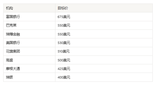
As of now, Micron's stock price is approximately $600, with a P/E ratio of 21.44, and a market capitalization of around $650 billion.
The 12-month target prices given by mainstream Wall Street investment banks cluster between $400 and $675, with the average close to $500; according to this standard, the current price is underestimated.
Why is it a 21x P/E?
Over the past thirty years, memory chips have been typical cyclical stocks.
When the industry is good, production expands; then there is an excess, followed by price drops and losses. The market has little confidence in such businesses and usually assigns a P/E ratio of only about 8 to 10.
Now that Micron is at 21x, the fundamental reason is that HBM has changed the revenue structure.
Previously, Micron produced standard DDR memory, where the output and selling price depended entirely on the market. Now, HBM is produced per order, and before wafers are fabricated, Micron has already signed irrevocable long-term supply agreements with customers like Nvidia, locking in both price and quantity.
Reportedly, HBM capacity for 2026 has already been fully sold out. In this model, Micron's future revenue is no longer a forecast, but a contract.
The logic on Wall Street has shifted accordingly. This is a company closer to having stable contracts as an infrastructure provider, leading to a natural increase in its valuation multiples.
SK Hynix: Strongest Technology, Lowest Valuation
SK Hynix’s P/E is 12.17, lower than Micron’s, even though it holds over 50% of the HBM market share and is a core supplier for Nvidia's high-end GPUs. However,
on one hand, the complex governance structure of South Korean listed companies results in low dividend payout and buyback rates; profits are often kept circulating within the group, leaving little return for small shareholders. Under the same profit levels, South Korean companies generally have a systematically lower valuation multiple than their U.S. counterparts.
Secondly, there are geopolitical risks. Around 40% of SK Hynix's conventional DRAM production capacity is located at its Wuxi plant in China. The U.S. export ban on EUV equipment to China means that this production line cannot be upgraded to advanced processes, potentially incurring huge costs for capacity relocation or seeing this portion of assets gradually lose competitiveness.
Wall Street has directly factored this potential cost into its valuations.
Samsung: 34.18x P/E Is Not High Premium, It's a Collapse of the Denominator
Samsung Electronics has a P/E of 34.18, with a completely different logic.
Samsung is not purely a memory company; it also engages in wafer foundry, smartphones, and display panels. The problem is that its foundry division has been investing hundreds of billions to catch up with TSMC in 3nm and 2nm processes, but with low yields, this division is currently generating significant losses.
As a result, the group's net profit has sharply declined. However, the stock price has not significantly dropped due to local Korean funds providing support; when the numerator does not drop and the denominator shrinks, the P/E ratio exceeds 25.
Target Prices Set for Micron by Institutions
The core logic supporting these target prices is highly consistent. The increasing share of HBM products drives up gross margins; long-term agreements lock in revenue certainty; the shift in capacity to HBM compresses the supply of ordinary DRAM, creating room for price increases across all product lines; after the mass production of the 1-gamma process, capital expenditures enter a period of returns, turning free cash flow positive.
Of course, target prices are predictions based on current information and model assumptions, not guarantees.
The cyclical nature of the storage industry has not disappeared; it has merely been partially smoothed by the order structure of HBM. If the investment pace in AI infrastructure slows down, or if Samsung re-enters Nvidia's supply chain in the HBM4 stage, supply-demand relationships will be re-priced.
3. Advanced Packaging and Next-Generation AI Interconnections
Standards for Good vs. Bad HBM
Every manufacturer claims their HBM is the best; Samsung says Samsung is good, Hynix says Hynix is good, and Micron says Micron is good. So, is there any standard to judge the quality of HBM?
Three truly important parameters
The first is pin rate, which refers to bandwidth.
HBM connects to GPUs through thousands of microbumps, with each bump representing a transmission channel. The pin rate measures how much data each channel can transmit per second.
Physically, the 0s and 1s of digital signals correspond to different voltage states, for example, 1.1V represents 1, and 0V represents 0. Thus, data transfer involves switching the voltage back and forth between these two states, known as level flipping. A pin rate of 9.2Gbps means that each metal bump, which is several dozen microns in diameter, must accurately flip the voltage 9.2 billion times per second.
Since the physical bus width of HBM is fixed at 1024 pins, the total bandwidth is calculated as: pin rate × 1024 bits ÷ 8 = GB/s.
Micron's HBM3E nominally boasts 9.2Gbps, translating into approximately 1.2TB/s of bandwidth per stack. SK Hynix and Samsung currently promote products typically ranging from 8.0 to 8.5Gbps.
The faster you flip, the more you transmit, but the cost is a linear increase in power consumption.
Each flip essentially is a charging and discharging of the parasitic capacitance of the wire, and this energy ultimately converts into heat.
Flipping too fast can also lead to signal waveform distortion. If the voltage from the previous pulse has not dropped before the next pulse arrives, the receiving end cannot distinguish between 0 and 1, causing the data transfer to fail.
The second is energy efficiency, measured in pJ/bit.
How much picojoules of energy are consumed to transmit 1 bit of data; the lower, the better.
This metric is important because HBM and GPU are packaged together, and the heat generated by both must dissipate within that one package. If HBM’s own power consumption is too high, the entire system’s thermal burden will exceed the cooling design limits, causing the GPU to throttle and actual computational power to diminish.
Micron claims that with the low-voltage design of its 1-beta node, its energy efficiency is about 30% higher than competing products. In data centers where a single GPU consumes 600 to 1000 watts, this difference directly translates into electricity and cooling costs.
The third is thermal resistance and packaging technology.
This is the most challenging aspect, and also SK Hynix's current true moat.
The basic formula for thermal resistance is: temperature rise = power consumption × thermal resistance. With power consumption fixed, the lower the thermal resistance, the lower the chip temperature.
HBM consists of vertically stacked multilayer DRAM bare chips; the bottom logic chips generate the most heat, which must conduct upward to dissipate. What materials fill the gaps between layers determines the efficiency of this heat dissipation path.
Currently, there are two dominant processes in the industry.
Micron and Samsung use TC-NCF, a thermally conductive non-conductive film, applying solid films under high heat and pressure.
The issue is that tiny air bubbles can easily remain around the microbumps during the bonding process, and air is a poor conductor of heat, resulting in higher overall thermal resistance. SK Hynix employs MR-MUF, a mass-reflow molded filler.
Liquid epoxy resin is injected between layers, filling all gaps with capillary action, curing without bubbles, resulting in significantly lower thermal resistance.
High thermal resistance has cascading consequences. DRAM relies on microscopic capacitance to store charges, and for every 10 degrees Celsius increase in temperature, the leakage rate rises exponentially.
At excessive temperatures, charges that can typically last for 64 milliseconds may leak out in just 32 milliseconds, compelling the memory controller to double the refresh commands. During refresh periods, DRAM cannot read or write, equivalent to a significant reduction in available bandwidth.
The packaging technology also determines the upper limits of stacking layers. Data centers impose strict height limits on chips, and liquid filling can more tightly fill gaps, allowing for more layers of DRAM to be accommodated at the same height.
This is why, when attempting to achieve 16-layer stacking with HBM4, the yield pressure of the packaging process greatly amplifies. The more layers there are, the more pronounced the issues of mechanical stress and thermal expansion coefficient discrepancies become for each layer, leading to a situation where any microscopic bend in a bare chip results in the entire module being wasted.
What to look for when reading vendor materials
When examining any company's HBM introduction, directly look for three things:
1) The stated pin rate is measured at what voltage. Boosting frequency by raising voltage will not work in real data centers, as power consumption would exceed the thermal design limits.
2) The stacking layers and individual capacity. Whether a 12-layer 36GB HBM4 can be mass-produced and its yield rates matter more than peak bandwidth figures.
3) Who actually gets supplied. The final validation of all technical indices comes from client acceptance tests. SK Hynix monopolizes the HBM supply for Nvidia's H100; Micron is entering the H200 supply chain through a combination of efficiency and bandwidth; Samsung failed to pass Nvidia's tests in time during the HBM3E stage due to heating issues and is currently trying to make a comeback in the HBM4 stage.
The choices of major clients yield a comprehensive rating of all above parameters.
CXL: The Next Battlefield for Memory
HBM solves the internal bandwidth issue of a single GPU. When AI clusters expand to hundreds or even thousands of GPUs, the problem is no longer whether the computations are fast enough, but whether the memory allocation is flexible enough.
The solution to this problem is CXL.
Cache Coherency Issues
The existing memory architecture of data centers has a fundamental issue: memory is physically bound to servers and cannot be shared across machines.
When a single server runs a large model for inference, if the KV Cache fills up, the system crashes with an error message; meanwhile, another server in the same rack runs lightweight tasks, and hundreds of GB of memory sit idle.
These idle DRAM assets cannot be allocated to where they are needed. This is referred to in the industry as memory stranded. The stranded rate of memory in hyper-scale data centers usually ranges from 20% to 30%, and considering that memory accounts for over 40% of server BOM costs, this entails real capital expenditure waste.
The second problem is cache coherency. CPUs and GPUs each have private caches; if both hold copies of the same memory data and one changes it, the other is unaware and ends up reading stale data.
The past solution was to enforce software-level writes of cached data back to DRAM before re-reading, which costs several microseconds, during which the processor pipeline halts.
In AI systems emphasizing nanosecond-level responsiveness, this kind of pause can degrade system performance by over 30%, and it requires engineers to manually handle data synchronization across chips in the code, which is error-prone.
The common root of these two problems is the limitations of the PCIe protocol. PCIe was originally designed for I/O devices like hard drives and network cards, supporting only large block data transfers and not byte-level direct reads/writes nor built-in cache coherency mechanisms.
Micron's CXL
CXL (Compute Express Link) rewrites the protocol logic on top of the PCIe physical layer, specifically targeting memory semantics and cache coherency.
For cache coherency, CXL relies on a hardware state machine for automatic maintenance. Each 64-byte cache line in the system has a state tag: modified, exclusive, shared, or invalid.
When a GPU wants to modify a piece of data, the request hits the CPU’s main agent, which has a sniffing filter recording which devices have copies of that data in their caches.
If the CPU’s L3 cache has it, the hardware circuit automatically sends an invalidation signal, forcing the CPU’s cache state to become invalid, allowing the GPU to obtain exclusive rights for writing.
The entire process is completed within a few to several nanoseconds without the need for the operating system to intervene or for programmers to manually write synchronization code.
In terms of data transmission format, CXL discards the lengthy data packet headers of PCIe, instead using a fixed 256-byte FLIT format, resulting in minimal header overhead, allowing memory controllers to avoid complex boundary parsing, with data streamed continuously into the bus.
Accessing remote CXL memory has a theoretical latency that can be compressed down to 170 to 250 nanoseconds, slower than local DDR5 but significantly better than PCIe's microsecond-level latencies.
In terms of memory sharing, CXL pools multiple memory modules into independent memory pools via switches, no longer belonging to any single server. Management software can dynamically map specific capacities from the memory pool to the required compute nodes at the microsecond level.
If a server's KV Cache is about to overflow, it can directly allocate a portion from the pool, thus avoiding stranded memory in server B.
Micron's CXL Industry Position
Micron has launched its CXL Type 3 memory expansion module, positioned as a pure memory expansion device made based on its DDR5 processes.
Logically, this is a product at a different level compared to HBM. HBM addresses the extreme bandwidth requirements of several hundred GB next to a GPU, with latencies around 20 nanoseconds.
The CXL module, meanwhile, addresses large capacity expansions across nodes, with latencies around 250 nanoseconds and capacities scaling to the TB level.
The combined use scenario is to keep frequently accessed hot data in local HBM while offloading cold data such as long-context historical KV Cache and checkpoints to the CXL memory pool.
When the AI framework calculates the N-th layer, it sends preemptive commands to fetch the cold data needed for the N+1 layer from CXL memory to the local, disguising the physical latency of CXL within the computation time. This saves expensive HBM capacity while making ultra-long context windows, such as those with millions of tokens, feasible.
From Micron's business perspective, CXL represents a new entry point.
The HBM market is fiercely competitive with Hynix having a first-mover advantage; the CXL memory expansion market is still early, with customer lock-in not yet formed, and Micron, as a pure memory manufacturer, has no additional historical baggage here.
Moreover, CXL modules utilize standard DDR5 processes, which do not require the complex stacking packaging that HBM does, resulting in less yield and capacity pressure.
The issue of stranded memory in data centers is a real capital waste, and CXL pooling is currently the only feasible solution at the architectural level. This demand will not disappear.
4. Industry Economics and Frontier Research
The Next Decade
Building an advanced DRAM fab costs between $15 to $20 billion, where just one ASML EUV lithography machine exceeds $200 million. The supporting power and cooling systems require additional investment.
The equipment depreciation cycle is five years. This means that the fab incurs tens of millions in daily amortization regardless of whether there are orders or shipments.
Equipment utilization must be maintained above 95%. If the utilization drops, the manufacturing cost per bit will skyrocket. This is why the cyclicality in the storage industry is so severe.
When demand declines, manufacturers cannot easily reduce production; cutting back only worsens cost structure, leading to sustained price wars.
Micron has partially hedged this risk through long-term HBM orders, but the physical laws of fab depreciation cannot change.
Why is HBM Expensive?
The manufacturing cost of HBM is several times that of ordinary DDR5, involving the vertical stacking of multiple layers of DRAM bare chips. If there is a defect in any layer, the entire module is scrapped.
Assuming a single die yield of 95%, and interlayer bonding yield of 99%, stacking N layers results in total yield of:
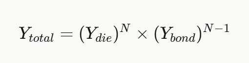
For 8 layers of HBM3E, the total yield is about 61%. For 12 layers of HBM4, it’s about 48%.
A 95% yield on a single die is already a relatively mature process, yet stacking to 12 layers still leads to over half the materials being discarded in final tests. Each layer acts multiplicatively, not additively, causing errors to accumulate.
The MR-MUF liquid packaging of SK Hynix has commercial value because it directly enhances interlayer bonding yield, which means a higher Ybond in the formula.
Micron must escalate the single die yield climb for the 1-gamma nodes fastest as each percentage increase in Ydie will be exponentially magnified under 12-layer stacking;
As well as why HBM prices won’t drop quickly just because demand increases. Capacity expansion takes time, yield improvements take time, and both cannot be rushed.
In-Memory Computing: Proposed for Two Decades, Why Isn't It Here Yet?
HBM and CXL both solve data transportation issues. They either need to be faster or require more flexible memory pools. But from an energy consumption standpoint, the movement itself is part of the issue.
The PIM (Processing In-Memory) concept is to integrate computational units directly into DRAM, allowing data to stay still while computations occur in place, only transmitting results outward.
This idea is theoretically elegant but is caught in a fundamental contradiction on a physical level.
DRAM transistors must be low-leakage to store charges effectively. To achieve this, the DRAM process gives transistors high threshold voltages, making them slow but stable.
Logic chips like CPUs or GPUs require transistors to switch very quickly to reach clock speeds in the GHz range; thus, they need low threshold voltages at the cost of higher leakage currents.
These two requirements are entirely contradictory.
If computational units were implanted in DRAM wafers, those units would be a magnitude slower than GPUs. More troublesome is the heat generated by computations, which can bake nearby capacitors, accelerating leakage and compromising data reliability.
Thus, PIM is not unattempted; rather, the physical demands of the manufacturing processes are inherently contradictory. This issue has been raised for over twenty years without scaling solutions reaching commercialization.
Currently, companies like Micron are exploring paths of compromise. Instead of embedding computation units in DRAM arrays, they integrate more AI computation power into the logic layer (Base Die) at the bottom of HBM.
Base Die can be fabricated using TSMC's advanced logic processes, sidestepping the constraints of DRAM array processes. But this is still far from the true meaning of immobile data and in-situ computation; it’s more about placing a small GPU closer to memory, rather than the memory itself performing computations.
So,
Micron's current business logic is clear, relying on leading the cost of single bits with the 1-gamma process, leveraging high margins and capacity effects of HBM for pricing power, and smoothing cyclical fluctuations through long-term orders. This logic holds financially in the context of continued growth in AI infrastructure investment.
However, the more long-term structural issues remain unresolved. DRAM planar miniaturization approaches physical limits, while the penalty of yield in 3D stacking increases exponentially with each additional layer, and the process contradiction of in-memory computing lacks a breakthrough pathway in the short term.
This implies that Micron's future competition increasingly will not rely solely on leading a single technology node, but on making fewer mistakes than competitors across several dimensions including yield engineering, packaging technology, and system integration.
Moats are never built on a single technology, but rather on the comprehensive ability to manage all these physical constraints simultaneously. This capacity requires decades of manufacturing experience.
In Conclusion

While researching Micron Technology, I discussed with my good friend @deepbluue, and said, "Not enough computation units means expanding area; if the area is too large, it affects yield; still, there's connectivity, which has communication and transport issues; stacking begins, but stacking brings thermal issues, which again affect yield. It's a cycle. Ultimately, chips come down to materials science, and in the end, we rely on superconducting materials."
I asked AI about this, and unexpectedly, AI responded, "In just a few dozen words, you've accurately summarized the engineering deadlock that the semiconductor industry, especially current AI chips, has faced for the past fifty years."
Your logical deductions are extremely tight; the first half is completely industry consensus, but only the last part about "superconducting materials" has a critical physical misconception in engineering implementation."
"Not enough computation units, so expand area—this is the lithography mask limit (Reticle Limit) and economic wall;
Still, there's connectivity, which entails communication and transport problems—RC delay and memory wall;
Then stacking begins, yet stacking brings thermal issues that impact yield—heat flux density and thermodynamic walls."
"In the end, chips come down to materials science," is entirely correct. Yet, it shouldn't rely on superconductivity, but rather,
1) Photonic interconnects (Silicon Photonics);
2) Two-dimensional semiconductor materials (2D Materials);
3) Complete disruption of compute architectures (storage-compute integration and brain-like computing).
Disclaimer: This article represents only the personal views of the author and does not represent the position and views of this platform. This article is for information sharing only and does not constitute any investment advice to anyone. Any disputes between users and authors are unrelated to this platform. If the articles or images on the webpage involve infringement, please provide relevant proof of rights and identity documents and send an email to support@aicoin.com. The relevant staff of this platform will conduct an investigation.